Make: Electronics (56 page)
Authors: Charles Platt

Fundamentals
Common part numbers
Each 14-pin chip can contain four 2-input gates, three 3-input gates, two 4-input gates, one 8-input gate, or six single-input inverters, as shown in the following table.
2 input | 3 input | 4 input | 8 input | |
AND | 7408 | 7411 | 7421 | |
NAND | 7400 | 7410 | 7420 | 7430 |
OR | 7432 | 744078* | ||
NOR | 7402 | 7427 | 744078* | |
XOR | 7486 | |||
XNOR | 747266 | |||
Inverter | (1 input) 7404 | |||
*The 744078 has an OR output and a NOR output on the same chip. |
Figures 4-66 through 4-74 show the internal connections of the logic chips that you are most likely to use. Note that the 7402 NOR gate has its logical inputs and outputs arranged differently from all the other chips.
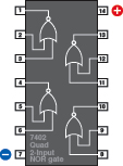
Figure 4-66.
Figures 4-66 through 4-74 show pinouts for some of the most widely used logic chips. Note that the inputs of the 7402 are reversed compared with the other chips.
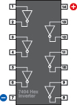
Figure 4-67
.
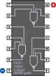
Figure 4-68
.
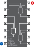
Figure 4-69
.
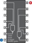
Figure 4-70
.
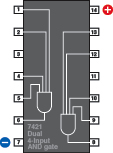
Figure 4-71
.
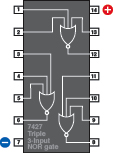
Figure 4-72
.
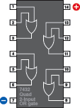
Figure 4-73
.
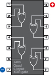
Figure 4-74
.
Fundamentals
Rules for connecting logic gates
Permitted:
- You can connect the input of a gate directly to your regulated power supply, either positive side or negative side.
- You can connect the output from one gate directly to the input of another gate.
- The output from one gate can power the inputs of many other gates (this is known as “fanout”). The exact ratio depends on the chip, but you can always power at least ten inputs with one logic output. The output from a logic chip can drive the trigger (pin 2) of a 555 timer. The output from the timer can then deliver 100mA, easily enough for half-a-dozen LEDs or a small relay.
- Low input doesn’t have to be zero. A 74HCxx logic gate will recognize any voltage up to 1 volt as “low.”
- High input doesn’t have to be 5 volts. A 74HCxx logic gate will recognize any voltage above 3.5 volts as “high.”
See Figures 4-75 and 4-76 for a comparison of permitted voltages on the input and output side of 74HCxx and 74LSxx chips.
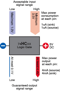
Figure 4-75.
Each family of logic chips, and each generation in each family, has different standards for input and output minimum and maximum voltages. This diagram shows the standards used by the HC generation of the CMOS family, which was chosen for most of the projects in this book. Note that the current required for input is minimal compared with the current available for output. The power supply to the chip makes up the difference.
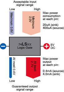
Figure 4-76.
Because the LS generation of the TTL family has such different tolerances for input voltages and different standards for output voltages, the LS generation of TTL chips should not be mixed in the same circuit as the HC generation of CMOS chips, unless pull-up resistors are used to bring the LS chips into conformance with standards expected by the HC chips. See
Experiment 21
for a case study in using LS chips.